Debugger Buddy
(previously called the Circuit Solver)
To simplify the distribution of information regarding the Debugger Buddy, I have consolidated all necessary files into a download available here:
At this time, I have not made the 3D models for the project available because they are incomplete and still need some revisions to make them work as well as I feel they should.
I have left the original content of this page available below, however, much of it is likely outdated and will be removed completely once a description video for this project is posted on my YouTube channel.
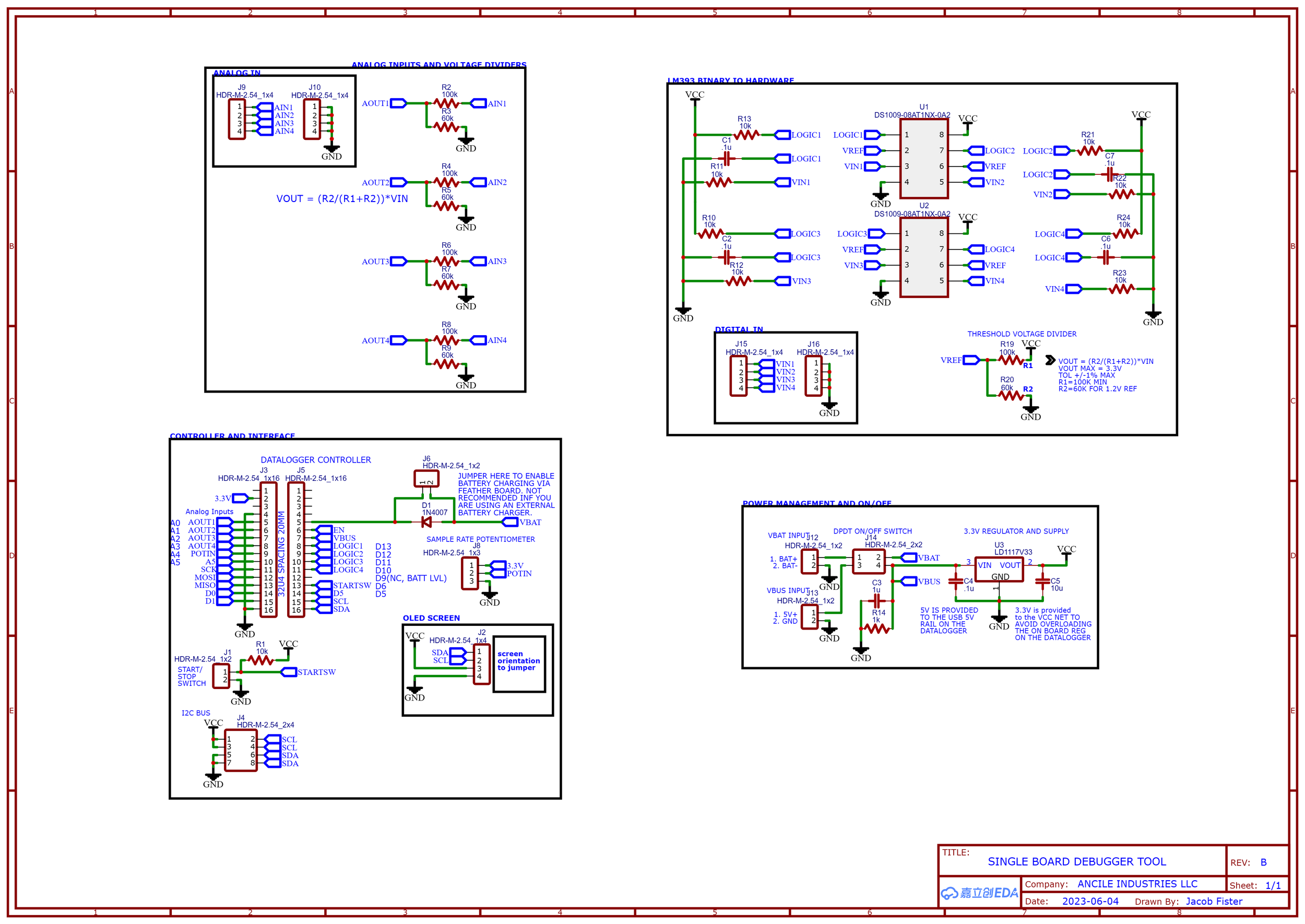
The Circuit Solver (real name TBD) v1.0 was designed to both give real-time information on circuits as well as log data to an SD card at different frequencies. Maintaining the device status as being widely applicable, customizable, and flexible was a priority during design. The primary use case for this device is to test and log circuit behavior for evaluation of parts and components, but given the flexibility of the design, exact usage can vary greatly from user to user.
The Circuit Solver Motherboard (CSM) consists of the analog input, digital input, battery and power interface. The secondary board houses the microcontroller socket, and OLED screen mounting point. The actual power supply, batteries, and charge circuit are separate and are a part of what’s called the Circuit Solver Reference Version (CSRV).
The CSRV is the device as-built by Ancile Industries LLC, utilizing additional hardware that will also be listed in this document in order to make the device a finished product. The final product CSRV is a portable logic analyzer-type tool with long battery life.
The digital inputs are routed through 2 LM393 ICs yielding a total number of 4 inputs. The LM393 chips can take a maximum input of 35V, though it is recommended not to approach that limit and to stay under 30V to maximize the life of the IC. The default state for the output of the LM393 is HIGH when there is no input, and LOW when the input is HIGH.
The trigger or threshold voltage is set by a voltage divider, whose value by default on the CSRV outputs about 1.2 volts. This can also be changed to any voltage by adjusting the resistor values of the voltage divider. If an adjustable threshold is desired, simply use a potentiometer in place of the resistors.
When an input above 1.2V (or other custom threshold value) is supplied to the LM393, the ICs output is pulled LOW. When the input to the LM393s is below the threshold value, the output of the IC goes HIGH. Take care to take this into account when programming your Circuit Solver.
Analog
The analog section of the circuit is composted of 4 voltage dividers. On the CSRV the default range is 0-5V for the inputs. The 100k and 60k resistors on the voltage dividers take the 5V down to 3.125V in perfect conditions. However, given resistors have a tolerance depending on your selection, it is important to calibrate each input in the program and check against a voltmeter to ensure maximum accuracy.
[Calibration Instructions to be added soon]
Battery and Power
Power is provided to the board either via a battery system or through a USB connection. A USB connection should only be used if the battery connection is turned off. [A future revision of the board will have isolation circuitry or hardware to automatically cut power from the batteries in the event a USB is connected while it is turned on or to block the connection of a USB cable unless the power switch is in the off position.
The capacitor [C3] and resistor [R14] (R14 should be at least 100k, picture is in error)*** are provided in order to give a large enough current draw from the USB rail of an IP5328P charge board to initiate power to the board’s output. A capacitor should only be added if the circuit will not turn on with existing load, and the resistor should only be added if the capacitor is not enough. It is recommended to start with the smallest capacitor available and work up until the circuit turns on reliably.
5V from the circuits USB rail is provided to the 3.3V regulator.
The Circuit Solver consists of 4 analog inputs, 4 digital inputs, a socket for the microcontroller (v1.0 using the M0 datalogger from Adafruit, the 32u4 version can be used if a smaller program with fewer variables is used), a display screen, rechargeable power supply for mobile operation, and a built-in power supply with PWM capability. The built-in power supply uses the mPSU board also produced by Ancile Industries LLC.
The analog inputs are routed through voltage dividers before continuing to the microcontroller. This is done to enable the Circuit Solver to read relatively high voltages without damaging the micro controller. The default analog input voltage limit is 5V for the CSRV, but each input can be configured individually to enable a wide range of input and precision to be utilized.
The microcontroller selected for this is a 32u4 based datalogger from Adafruit. The reason for this selection is the built-in SD card reader/writer, and the ability to charge an external Li-Ion cell (separate charging circuit is used in the reference design) Future versions will use the M0 datalogger board to enable faster recording speeds (48MHz on the M0, 8MHz on the 32u4) since power is not a concern. It is possible to use the M0 based microcontroller on the current design, as long as the pinout is the same. At the time this document was written, the Adafruit boards pinout for both controllers are the same.
A standard OLED SSD1306 display connected via I2C is used to display pertinent information on the inputs, battery level, and system status.
The battery system is comprised of 1 or more 3.7V Li-Ion cells in parallel connected to an IP5328P-based charge board for 1S#P charging applications. The power supply and CSRV are powered off of separate 5V rails.
Digital and VREF
The digital signals provided to the Circuit Solver (VIN#) are connected to the LM393 input pins. The LM393 ICs compare the VIN voltage to the reference voltage and output a HIGH signal. Once the input is pulled HIGH, this activates a transistor that opens to ground and pulls BIN# LOW. This signal is the one read by the microcontroller. [The section with the transistors will most likely be removed or revised to use faster responding transistors, or to read the output from the LM393s directly instead of indirectly passing through transistors. Alternate transistors can also be used in this design, ignoring the designation on the schematic.]
The reference voltage is selected by choosing resistors for the voltage divider that will achieve the desired output starting from a voltage input of 3.3V. A potentiometer can also be used to make the threshold voltage adjustable. [A future revision of the design will most likely include a connection between the reference voltage and an analog pin to enable displaying the current VREF value on a screen. This can also be achieved by using a secondary Arduino or other microcontroller that is used just to read various values and display them on a second screen, bypassing the need to modify the current circuit board of the CSRV.]
June 2023 Update
Upon further testing and review of the LM393 datasheet, I determined that using the 2N2222 transistors hampered performance too much and was not required for this design. I removed the transistors and supporting components and was able to shrink the design.
Another affect that removing the transistors had is sped up the maximum frequency considerably. Reaction times of the transistors reached into the milliseconds, a MUCH slower operating speed than the microsecond-level reaction times of the LM393 chips.
I also reverted back to a single-board design from the split board design I used previously. Given the lower number of components, I decided it was better to have a simpler assembly than the marginal flexibility having a dual board design added at the cost of increased complexity. This should theoretically reduce the amount of noise introduced to the system.
The CSRV was also changed to no longer include a battery bank function with separate charge circuit, and instead will only use a battery large enough to operate the board itself for an extended period of time. In the future, a design will likely be developed that uses the mPSU design to give wireless power supply functionality, but it will most likely utilize an external power bank due to their wide availability, low cost, broader use-case and reliable functionality. Users will most likely already have one on hand, and if they do not, obtain one for a lower cost than purchasing the hardware required to construct that functionality on their own. A classic example of DIY or BUY, where the benefits of the “buy” option outweigh the “DIY” option. Ultimately, it will simply be more user friendly to utilize an external power source than to add a most-likely redundant one into the CSRV.
The last notable change in the design is that I double the width of all traces. At the voltage and current levels this board sees, it probably won’t make much of a difference, but in an effort to maximize the speed at which this board can run, it was a simple and cost-free change to make to decrease the bottleneck potential of that variable. The updated board and schematic is shown below.
Also, I’ve named this version the Debugger Buddy.
=)